| CPC H01L 29/42336 (2013.01) [H01L 29/407 (2013.01); H01L 29/66734 (2013.01); H01L 29/66825 (2013.01); H01L 29/788 (2013.01); H01L 29/7813 (2013.01)] | 13 Claims |
|
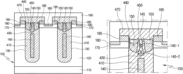
1. A trench metal-oxide semiconductor field-effect transistor (MOSFET) comprising:
a substrate;
a body region, formed on the substrate;
a source region, disposed in the body region;
a gate trench, formed on the substrate;
a lower electrode, formed in a lower region of the gate trench;
a plurality of upper electrodes, formed above the lower electrode, wherein the plurality of upper electrodes comprises: a first upper electrode, formed to overlap the lower electrode; and second upper electrodes, configured to surround the first upper electrode;
a first inter-electrode insulating layer, formed between the lower electrode and the first upper electrode;
a gate insulating layer, formed on a sidewall of the gate trench;
an interlayer insulating layer, formed on the plurality of upper electrodes; and
a source metal, provided on the interlayer insulating layer, and configured to be in contact with the body region.
|