| CPC H01L 29/2003 (2013.01) [H01L 23/14 (2013.01); H01L 23/31 (2013.01); H01L 23/36 (2013.01); H01L 23/5226 (2013.01); H01L 23/53228 (2013.01); H01L 27/088 (2013.01)] | 20 Claims |
|
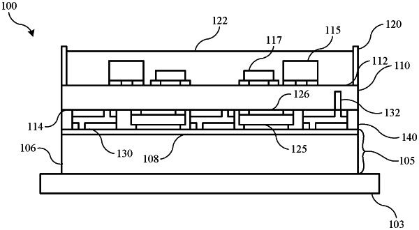
1. An integrated power module comprising:
a printed circuit board characterized by a first surface and a second surface, and including a thermal via extending from the second surface towards the first surface;
one or more surface-mounted components coupled with the first surface of the printed circuit board;
a heat-transfer substrate;
one or more gallium nitride transistors coupled between and soldered to each of the second surface of the printed circuit board and the heat-transfer substrate; and
a spacer coupled between and soldered to each of the printed circuit board and the heat-transfer substrate, wherein the spacer is directly coupled to the thermal via.
|