US 11,862,685 B2
Wafer and method of manufacturing wafer
Jong Hwi Park, Cheonan-si (KR); Kap-Ryeol Ku, Cheonan-si (KR); Jung-Gyu Kim, Cheonan-si (KR); Jung Woo Choi, Cheonan-si (KR); and Myung-Ok Kyun, Cheonan-si (KR)
Assigned to SENIC INC., Cheonan-si (KR)
Filed by SENIC Inc., Cheonan-si (KR)
Filed on Feb. 4, 2022, as Appl. No. 17/665,166.
Application 17/665,166 is a division of application No. 17/355,663, filed on Jun. 23, 2021, granted, now 11,289,576.
Claims priority of application No. 10-2020-0086798 (KR), filed on Jul. 14, 2020.
Prior Publication US 2022/0157944 A1, May 19, 2022
Int. Cl. H01L 21/16 (2006.01); H01L 29/16 (2006.01); G01N 23/207 (2018.01); H01L 21/02 (2006.01); H01L 21/66 (2006.01)
CPC H01L 29/1608 (2013.01) [G01N 23/207 (2013.01); H01L 21/02529 (2013.01); H01L 22/12 (2013.01)] 8 Claims
OG exemplary drawing
 
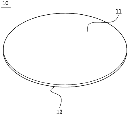
1. A wafer having a retardation distribution measured with a light having a wavelength of 520 nm,
wherein an average value of the retardation is 38 nm or less,
wherein the wafer comprises a micropipe, and
wherein a density of the micropipe is 1.5/cm2 or less.