| CPC H01L 29/1608 (2013.01) [H01L 21/02002 (2013.01); H01L 21/02378 (2013.01)] | 6 Claims |
|
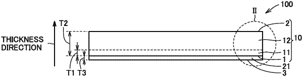
1. A recycle wafer of silicon carbide comprising:
a silicon carbide substrate having a first main surface and a second main surface opposite to the first main surface; and
a first silicon carbide layer in contact with the first main surface, wherein
the silicon carbide substrate includes a substrate region that is within 10 μm from the first main surface toward the second main surface, and
in a direction perpendicular to the first main surface, a value obtained by subtracting a value that is three times a standard deviation of a nitrogen concentration in the substrate region from an average value of the nitrogen concentration in the substrate region is greater than a minimum value of a nitrogen concentration in the first silicon carbide layer.
|