| CPC H01L 29/1037 (2013.01) [H01L 29/0673 (2013.01); H01L 29/165 (2013.01); H01L 29/41775 (2013.01); H01L 29/42392 (2013.01); H01L 29/66795 (2013.01); H01L 29/785 (2013.01); H01L 21/02532 (2013.01); H01L 21/02636 (2013.01); H01L 21/26513 (2013.01); H01L 21/308 (2013.01); H01L 21/30604 (2013.01); H01L 21/31116 (2013.01); H01L 29/6653 (2013.01); H01L 29/6656 (2013.01); H01L 29/66545 (2013.01); H01L 29/66553 (2013.01); H01L 29/7848 (2013.01)] | 20 Claims |
|
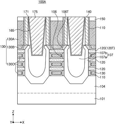
1. A semiconductor device, comprising:
a substrate, the substrate including an active region extending in a first direction;
a plurality of channel layers on the active region, the plurality of channel layers disposed in a direction perpendicular to an upper surface of the substrate;
a gate electrode respectively surrounding the plurality of channel layers, the gate electrode extending in a second direction crossing the first direction, the gate electrode including a first portion and a second portion on an uppermost channel layer of the plurality of channel layers, the first portion of the gate electrode being on the second portion of the gate electrode, the gate electrode further including a silicon cap layer between the first portion and the second portion of the gate electrode; and
a source/drain structure disposed on both sides of the gate electrode, respectively, and connected to each of the plurality of channel layers,
wherein the second portion of the gate electrode overlaps the source/drain structure in the first direction to provide an overlapped portion of the gate electrode.
|