| CPC H01L 29/0847 (2013.01) [H01L 21/823814 (2013.01); H01L 21/823821 (2013.01); H01L 27/0924 (2013.01); H01L 29/41791 (2013.01); H01L 29/785 (2013.01); H10B 10/12 (2023.02); H10B 12/36 (2023.02)] | 11 Claims |
|
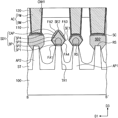
1. A semiconductor device, comprising:
a substrate including a plurality of active fins that are adjacent to each other;
a gate electrode running across the plurality of active fins;
a source/drain pattern adjacent to one side of the gate electrode and on the plurality of active fins;
an active contact electrically connected to the source/drain pattern; and
a silicide layer between the source/drain pattern and the active contact,
wherein:
the source/drain pattern includes:
a body part including a plurality of first semiconductor patterns respectively on the plurality of active fins, a second semiconductor pattern on the plurality of first semiconductor patterns and connecting the plurality of first semiconductor patterns to each other, and a third semiconductor pattern on the second semiconductor pattern; and
a capping pattern on the body part,
the body part has a first facet, a second facet on the first facet, and a first corner edge defined where the first facet meets the second facet,
the first corner edge protrudes parallel to the substrate,
the first facet, the second facet and the first corner edge are adjacent to an outermost one of the plurality of active fins,
the capping pattern covers the second facet and exposes the first facet and the first corner edge,
the body part further has a third facet, a fourth facet on the third facet, and a second corner edge defined where the third facet meets the fourth facet,
the second corner edge protrudes parallel to the substrate,
the source/drain pattern has a maximum width between the first corner edge and the second corner edge,
the capping pattern includes a first segment on the second facet, a second segment on the third facet, and a third segment on the second corner edge,
the third segment is between the first segment and the second segment and connects the first and second segments to each other,
a maximum thickness of the first segment is greater than a maximum thickness of the third segment, and
a maximum thickness of the second segment is greater than the maximum thickness of the third segment.
|