| CPC H01L 29/0642 (2013.01) [H01L 29/0649 (2013.01); H01L 29/7397 (2013.01); H01L 29/7813 (2013.01); H01L 29/7831 (2013.01)] | 14 Claims |
|
1. A semiconductor device, comprising:
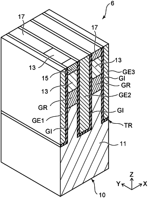
a semiconductor part including a first semiconductor layer of a first conductivity type, a second semiconductor layer of a second conductivity type, a third semiconductor layer of the first conductivity type, and a fourth semiconductor layer of the second conductivity type, a plurality of trenches provided at a front side of the semiconductor part;
a first region partially provided between the first semiconductor layer and the second semiconductor layer, the first region being provided between the first semiconductor layer and the third semiconductor layer, the first region including a material having a lower thermal conductivity than the first semiconductor layer;
a first electrode provided at the front side of the semiconductor part; and
a plurality of control electrodes provided in the plurality of trenches, respectively, the plurality of control electrodes each being electrically insulated from the semiconductor part via an insulating film, the plurality of control electrodes including a first control electrode, and a second control electrode next to the first control electrode,
the second semiconductor layer being provided between the first semiconductor layer and the first electrode, the second semiconductor layer being provided between the first and second control electrodes, the second semiconductor layer facing the first and second control electrodes via the insulating film,
the third and fourth semiconductor layers being provided between the second semiconductor layer and the first electrode, the third and fourth semiconductor layers being electrically connected to the first electrode and arranged along a front surface of the second semiconductor layer facing the first electrode
the first region being provided continuously between two adjacent ones of the plurality of trenches, and
the first region being partially and discontinuously provided along a direction in which the trenches extend.
|