| CPC H01L 29/063 (2013.01) [H01L 21/823481 (2013.01); H01L 21/823493 (2013.01); H01L 27/088 (2013.01); H01L 29/0634 (2013.01); H01L 29/1095 (2013.01); H01L 29/66681 (2013.01); H01L 29/7816 (2013.01); H01L 29/7835 (2013.01); H03K 19/018507 (2013.01); H01L 21/823418 (2013.01); H01L 21/823892 (2013.01); H01L 27/0922 (2013.01); H01L 29/0696 (2013.01); H01L 29/0847 (2013.01); H01L 29/0886 (2013.01); H01L 29/404 (2013.01); H01L 29/42368 (2013.01)] | 20 Claims |
|
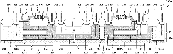
1. An integrated circuit (IC) comprising:
a substrate;
a termination device well in the substrate and having a first doping type;
a switching device bordering the termination device well on the substrate, wherein the switching device comprises a pair of source/drain regions and a gate electrode between the pair of source/drain regions;
a peripheral well in the substrate and having a second doping type opposite the first doping type, wherein the peripheral well is spaced from the pair of source/drain regions of the switching device and separates and individually surrounds the switching device and the termination device well;
a high side well overlying the termination device well in the substrate and having the second doping type, wherein the high side well has a sidewall boundary directly contacting the termination device well continuously in a first closed path;
a dielectric structure sunken into the substrate;
a spiral structure overlying the switching device and the dielectric structure; and
a contact region overlying the termination device well in the substrate and having the first doping type, wherein the contact region is spaced from the high side well and extends along the sidewall boundary continuously in a second closed path, and wherein the dielectric structure is continuous linearly from the contact region to the spiral structure.
|