| CPC H01L 29/063 (2013.01) [H01L 29/1095 (2013.01); H01L 29/66681 (2013.01); H01L 29/7816 (2013.01)] | 7 Claims |
|
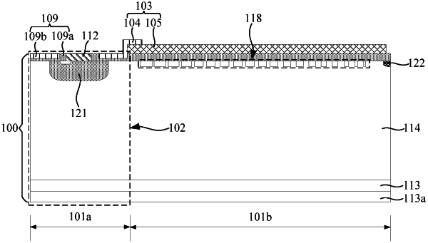
1. A method of making a high voltage semiconductor device comprising a combined junction terminal protection structure with a ferroelectric material, characterized by:
the method comprises:
providing a semiconductor wafer for preparation, the semiconductor wafer comprising a substrate, the substrate being formed with an active area, and the active area being formed with a partial structure of the high voltage semiconductor device;
depositing a ferroelectric material on the substrate, and performing rapid thermal annealing on the ferroelectric material, so as to crystalize the ferroelectric material;
patterning the ferroelectric material to form a ferroelectric material layer;
forming a remaining partial structure of the high voltage semiconductor device both in and on the active area, and at the mean time forming a first biasing field plate, the first biasing field plate being positioned on the ferroelectric material layer and in contact with the ferroelectric material layer, the first biasing field plate being electrically connecting to the active area, and a RESURF structure of a combined junction terminal protection structure being comprised of the ferroelectric material layer and a first biasing voltage,
wherein the ferroelectric material layer comprises hafnium dioxide-based material doped with aluminum and zirconium.
|