| CPC H01L 29/0607 (2013.01) [H01L 29/7816 (2013.01)] | 3 Claims |
|
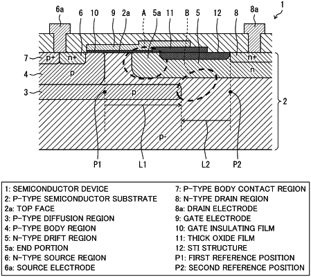
1. A semiconductor device, comprising:
a semiconductor substrate of a first conductivity type;
a body region of the first conductivity type, the body region being formed in a surface layer of the semiconductor substrate;
a source region of a second conductivity type, the source region being formed in contact with the body region;
a drain region of the second conductivity type, the drain region being formed away from the body region;
a gate electrode formed between the source region and the drain region;
a drift region of the second conductivity type, the drift region being formed in contact with the drain region in the surface layer of the semiconductor substrate, and the drift region having an end portion between the body region and the drain region;
a buried oxide layer provided at least under an end portion, of the gate electrode, toward the drain region, the buried oxide layer being formed to be buried from a top face of the semiconductor substrate, and the buried oxide layer being configured to alleviate an electric field; and
a semiconductor region of the first conductivity type, the semiconductor region being formed in a position deeper than the body region in order to have contact with a bottom face of the body region,
wherein, the semiconductor region is formed to extend in a direction along the top face of the semiconductor substrate,
a first distance is in a direction from a first reference position below an end, of the body region, toward the drain region to an end of the semiconductor region, the first distance being along the top face of the semiconductor substrate,
a second distance is in a direction from a second reference position below an end, of the drain region, toward the buried oxide layer to the end of the semiconductor region, the second distance being along the top face of the semiconductor substrate, and
the first distance and the second distance are set so that an intensity of 0.35 MV/cm or less is observed in an electric field of a first region including the end portion of the drift region and in an electric field of a second region between the end of the semiconductor region and the drain region.
|