| CPC H01L 29/045 (2013.01) [H01L 29/1608 (2013.01); H01L 29/66068 (2013.01); H01L 29/781 (2013.01); H01L 29/7813 (2013.01)] | 11 Claims |
|
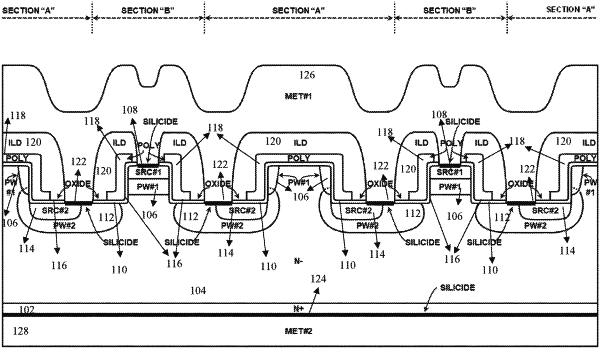
1. A device comprising a unit cell, the unit cell comprising:
a drift region and a source region of a first conductivity type;
a first well region and a second well region of a second conductivity type; and
a trench region that extends through the first well region,
wherein the source region is confined within the second well region,
wherein the second well region overlaps a portion of the first well region to form a composite well region, and
wherein the composite well region is interspersed between the trench region and the drift region.
|