| CPC H01L 29/04 (2013.01) [H01L 29/1033 (2013.01); H10B 12/00 (2023.02); H10B 53/30 (2023.02)] | 27 Claims |
|
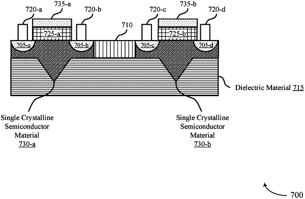
1. A method, comprising:
forming a cavity within a dielectric portion including one or more dielectric materials, wherein the cavity within the dielectric portion includes a taper from a first cross-sectional area toward a point;
depositing a semiconductor material in the cavity within the dielectric portion and above the one or more dielectric materials;
forming the semiconductor material in a single crystalline arrangement after depositing the semiconductor material in the cavity within the dielectric portion, wherein forming the single crystalline arrangement comprises nucleating the single crystalline arrangement based at least in part on heating and cooling the semiconductor material; and
forming a channel portion of a transistor based at least in part on doping the single crystalline arrangement of the semiconductor material.
|