| CPC H01L 28/92 (2013.01) [H01L 29/945 (2013.01); H10B 12/038 (2023.02); H10B 12/373 (2023.02)] | 21 Claims |
|
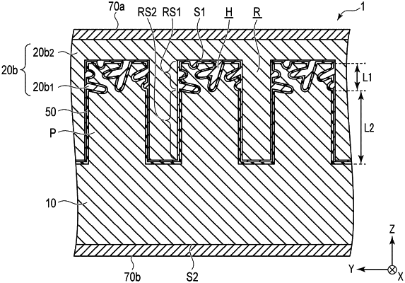
1. A capacitor comprising:
a conductive substrate having a first main surface and a second main surface and provided with a plurality of recesses on the first main surface, each of the recesses having a bottom between the first main surface and the second main surface, the conductive substrate further provided with a plurality of holes in one or more portions, wherein the one or more portions are each sandwiched between two adjacent ones of the plurality of recesses, and the conductive substrate is provided with the plurality of holes such that a top surface of each of the one or more portions has one or more of the plurality of holes and each of the one or more portions has a larger porosity in a region adjacent to an opening of the recess than in a region adjacent to a bottom of the recess;
a conductive layer covering the top surface, side walls and bottom surfaces of the plurality of recesses, and walls of the plurality of holes; and
a dielectric layer interposed between the conductive substrate and the conductive layer,. the dielectric layer being in direct physical contact with the top surface and entirely covering the top surface.
|