| CPC H01L 27/1469 (2013.01) [H01L 27/14634 (2013.01); H01L 27/14636 (2013.01)] | 10 Claims |
|
1. An imaging device comprising
an imaging element, and a semiconductor element provided to be opposed to the imaging element and electrically coupled to the imaging element, wherein
the semiconductor element includes:
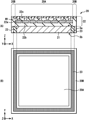
a wiring region provided in a middle portion and a peripheral region outside the wiring region;
a wiring layer having a wiring line in the wiring region;
a semiconductor substrate opposed to the imaging element with the wiring layer interposed therebetween and having a first surface and a second surface in order from a side of the wiring layer; and
a polishing adjustment section including a material that is lower in polishing rate than a constituent material of the semiconductor substrate, the polishing adjustment section being disposed in at least a portion of the peripheral region and provided in a thickness direction of the semiconductor substrate from the second surface.
|