US 11,862,660 B2
Pixel having two semiconductor layers, image sensor including the pixel, and image processing system including the image sensor
Jung-Chak Ahn, Suwon-si (KR)
Assigned to SAMSUNG ELECTRONICS CO., LTD., Suwon-si (KR)
Filed by SAMSUNG ELECTRONICS CO., LTD., Suwon-si (KR)
Filed on Jun. 7, 2021, as Appl. No. 17/340,273.
Application 12/684,163 is a division of application No. 11/524,695, filed on Sep. 21, 2006, granted, now 7,671,435, issued on Mar. 2, 2010.
Application 17/340,273 is a continuation of application No. 16/560,347, filed on Sep. 4, 2019, granted, now 11,152,419.
Application 16/560,347 is a continuation of application No. 16/285,686, filed on Feb. 26, 2019, granted, now 11,094,732.
Application 16/285,686 is a continuation of application No. 15/937,632, filed on Mar. 27, 2018, granted, now 10,249,677, issued on Apr. 2, 2019.
Application 15/937,632 is a continuation of application No. 15/047,444, filed on Feb. 18, 2016, granted, now 9,954,025, issued on Apr. 24, 2018.
Application 15/047,444 is a continuation of application No. 13/838,627, filed on Mar. 15, 2013, granted, now 9,293,501, issued on Mar. 22, 2016.
Application 13/838,627 is a continuation of application No. 12/684,163, filed on Jan. 8, 2010, granted, now 8,508,012, issued on Aug. 13, 2013.
Claims priority of application No. 10-2005-0091293 (KR), filed on Sep. 29, 2005.
Prior Publication US 2021/0296390 A1, Sep. 23, 2021
Int. Cl. H01L 27/146 (2006.01)
CPC H01L 27/14643 (2013.01) [H01L 27/1464 (2013.01); H01L 27/14612 (2013.01); H01L 27/14634 (2013.01); H01L 27/14636 (2013.01)] 20 Claims
OG exemplary drawing
 
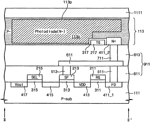
1. An image sensor comprising:
a first semiconductor substrate including a first surface and a second surface, at least one transistor formed on the first surface of the first semiconductor substrate;
a first insulating layer stacked on the at least one transistor;
a second semiconductor substrate having a first surface and a second surface,
a photodiode formed in the second semiconductor substrate;
a transfer gate pattern and a floating diffusion region of a transfer transistor formed on the first surface of the second semiconductor substrate;
a second insulating layer disposed between the first surface of the second semiconductor substrate and the first insulating layer;
wherein the first surface of the first semiconductor substrate and the first surface of the second semiconductor substrate face each other, and the first and second insulating layers are interposed between the first and second semiconductor substrates.