| CPC H01L 27/1464 (2013.01) [H01L 27/1465 (2013.01); H01L 27/14634 (2013.01); H04N 23/11 (2023.01); H04N 25/60 (2023.01); H04N 25/75 (2023.01)] | 12 Claims |
|
1. An infrared multispectral imaging sensor comprising:
a photosensitive backside-illumination detector (DET) that is made on a first substrate (100) made of InP, and having a backside face (101) and a frontside face (102), and that is formed of a matrix of pixels (105, P1, P2, P3) that are themselves made in a structure (103) based on InGaAs and deposited by epitaxy on the frontside face of the first substrate (100) made of InP; and
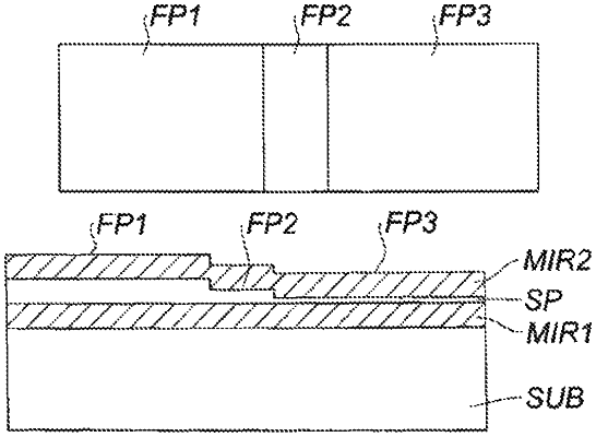
a filter module (MF) that is formed of a matrix of elementary filters (λ1, λ2, λ3) reproducing said matrix of pixels, and that is constituted by a stack made up of a first mirror (MIR1) and of a second mirror (MIR2) that are separated by a spacer (SP), said filter module defining a plurality of filter cells (IF11, IF12, . . . , IF44), each of which comprises at least two filters (FP1, FP2, FP3);
said infrared multispectral imaging sensor being characterized in that:
said filter module (MF) is formed on a second substrate (SUB) on which the first mirror (MIR1), the spacer (SP), and the second mirror (MIR2) have been deposited, in that order;
the second mirror (MIR2) is mounted into contact with said first substrate (100), thereby forming a hybrid multispectral imaging sensor that functions for wavelengths greater than 1000 nm and ranging up to 2200 nm; and
said first substrate (100) made of InP has a thickness less than 50 μm, and preferably less than 30 μm.
|