| CPC H01L 27/14636 (2013.01) [H01L 27/14618 (2013.01); H01L 27/14627 (2013.01); H04N 23/54 (2023.01)] | 20 Claims |
|
1. A semiconductor package comprising terminals,
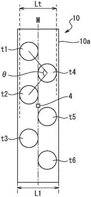
wherein the semiconductor package has a width and a length as viewed in plan, the length being greater than the width,
wherein, for any three terminals from among all of the terminals, an angle formed by two line segments connecting a center of gravity of a terminal positioned in a center in a longitudinal direction and a center of gravity of each of the other two terminals is 60° or more,
wherein the width L1 of the semiconductor package and a distance Lt between a rightmost end position of a terminal arranged at a rightmost end in a width direction of the semiconductor package among all of the terminals and a leftmost end position of a terminal arranged at a leftmost end in the width direction satisfy Lt/L1≥0.5,
wherein all of the terminals are spaced apart from a line segment passing through a center in the width direction of the semiconductor package with a first center of gravity of a first portion of all the terminals arranged on a first side across the line segment and a second center of gravity of a second portion of all the terminals other than the first portion arranged on a second side across the line segment,
wherein a number of terminals in the first portion and a number terminals in the second portion are equal, and
wherein the semiconductor package is a wafer level chip size.
|