| CPC H01L 27/14636 (2013.01) [H01L 24/16 (2013.01); H01L 24/48 (2013.01); H01L 27/1469 (2013.01); H01L 27/14627 (2013.01); H01L 27/14632 (2013.01); H01L 27/14634 (2013.01); H01L 27/14645 (2013.01); H01L 27/14685 (2013.01); H01L 27/14687 (2013.01); H01L 2224/16145 (2013.01); H01L 2224/48463 (2013.01); H01L 2924/146 (2013.01); H01L 2924/18161 (2013.01)] | 14 Claims |
|
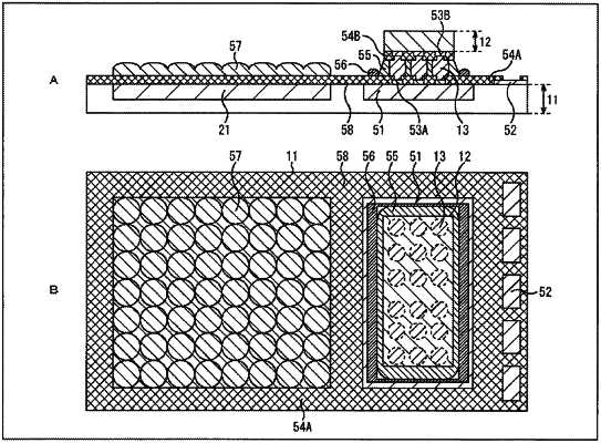
1. An imaging device, comprising:
a first semiconductor chip, wherein the first semiconductor chip includes a first semiconductor substrate and a plurality of arrays of pixels, and wherein the first semiconductor chip has a rectangular shape;
a second semiconductor chip, wherein the second semiconductor chip includes a second semiconductor substrate, wherein the second semiconductor substrate has a rectangular shape, wherein an area of the second semiconductor substrate is less than an area of the first semiconductor substrate, and wherein the second semiconductor substrate is disposed on a light receiving surface side of the first semiconductor substrate; and
a third semiconductor chip, wherein the third semiconductor chip includes a third semiconductor substrate, wherein the third semiconductor substrate has a rectangular shape, wherein an area of the third semiconductor substrate is less than the area of the first semiconductor substrate, and wherein the third semiconductor substrate is disposed on the light receiving surface side of the first semiconductor substrate,
wherein a first array of pixels included in the plurality of arrays of pixels is adjacent to at least a portion of the second semiconductor substrate, and
wherein a second array of pixels included in the plurality of arrays of pixels is adjacent to at least a portion of the third semiconductor substrate.
|