| CPC H01L 27/14636 (2013.01) [H01L 21/76898 (2013.01); H01L 23/481 (2013.01); H01L 27/1464 (2013.01); H01L 27/14643 (2013.01); H01L 27/14647 (2013.01); H04N 25/77 (2023.01); H04N 25/79 (2023.01); H01L 21/7682 (2013.01); H01L 2924/0002 (2013.01); H04N 25/75 (2023.01)] | 20 Claims |
|
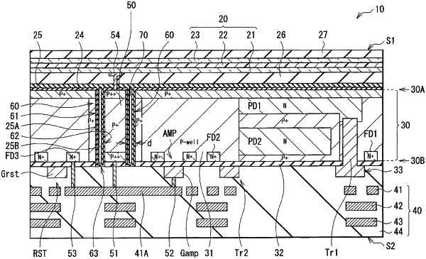
1. A solid-state imaging device, comprising:
one or more photoelectric conversion elements provided on and above a first surface of a semiconductor substrate;
a through electrode coupled to the one or more photoelectric conversion elements, and provided between the first surface and a second surface of the semiconductor substrate; and
a dielectric layer provided between the through electrode and the semiconductor substrate, provided above the through electrode extending along a surface of the one or more photoelectric conversion elements, and provided between the surface of the one or more photoelectric conversion elements and the first surface of the semiconductor substrate,
wherein the through electrode is made of a conductive material, and
wherein the dielectric layer is also provided along vertical side portions of the through electrode and includes an outer dielectric layer and an inner dielectric layer having a gap provided therebetween.
|