| CPC H01L 27/1463 (2013.01) [H01L 27/1464 (2013.01); H01L 27/14621 (2013.01); H01L 27/14623 (2013.01); H01L 27/14627 (2013.01); H01L 27/14636 (2013.01); H01L 27/14641 (2013.01); H01L 27/14645 (2013.01); H01L 27/14685 (2013.01); H01L 27/14689 (2013.01); H04N 25/75 (2023.01)] | 20 Claims |
|
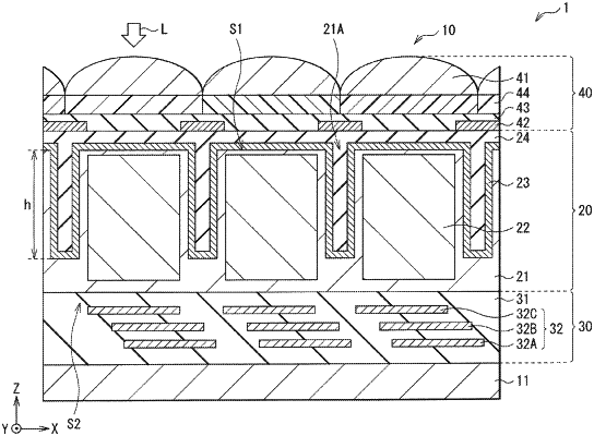
1. An imaging device, comprising:
a substrate including a photoelectric conversion region;
a first trench and a second trench, wherein the photoelectric conversion region is disposed between the first trench and the second trench;
a first film including silicon oxide disposed above the photoelectric conversion region at a light receiving surface side of the substrate and contacting the substrate;
a second film disposed above the first film at the light receiving surface side of the substrate;
a third film disposed above the second film at the light receiving surface side of the substrate; and
a fourth film disposed above the third film at the light receiving surface side of the substrate,
wherein the second film includes at least one of a group consisting of: hafnium oxide, zirconium oxide, aluminum oxide, titanium oxide, and tantalum oxide,
wherein the third film includes at least one of the group consisting of: hafnium oxide, zirconium oxide, aluminum oxide, titanium oxide, and tantalum oxide, and
wherein the fourth film includes at least one of the group consisting of: hafnium oxide, zirconium oxide, aluminum oxide, titanium oxide, and tantalum oxide.
|