| CPC H01L 27/14612 (2013.01) [H04N 25/531 (2023.01); H04N 25/532 (2023.01); H04N 25/75 (2023.01); H04N 25/771 (2023.01); H04N 25/78 (2023.01); H04N 25/79 (2023.01)] | 6 Claims |
|
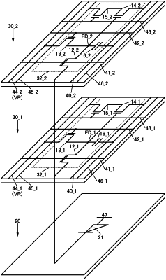
1. An operation method of an imaging device comprising;
obtaining first imaging data which is data corresponding to an illuminance of light emitted to a photoelectric conversion element and retaining the first imaging data in a first circuit in a first period,
obtaining second imaging data which is data corresponding to an illuminance of light emitted to the photoelectric conversion element and retaining the second imaging data in a second circuit in a second period, and
reading out the first imaging data retained in the first circuit and the second imaging data retained in the second circuit in a third period,
wherein a first layer comprising the photoelectric conversion element, a second layer comprising the first circuit, and a third layer comprising the second circuit are stacked in the imaging device.
|