| CPC H01L 27/124 (2013.01) [G06F 3/0412 (2013.01); G06F 3/0443 (2019.05); H01L 27/1259 (2013.01); G06F 2203/04103 (2013.01); G06F 2203/04107 (2013.01)] | 18 Claims |
|
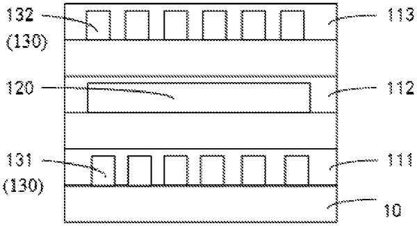
1. A display substrate having a display region and a pin region on a side of the display region, comprising:
a base substrate; and
at least one first signal line and at least one second signal line both on a side of the base substrate and both extending to the display region from the pin region;
wherein the display substrate further comprises a direct current (DC) conductive structure connected to a constant DC voltage, and
the DC conductive structure is between the at least one first signal line and the at least one second signal line and spaced apart from each of the at least one first signal line and the at least one second signal line,
the DC conductive structure has a stacked metal structure of titanium/aluminum/titanium (Ti/Al/Ti).
|