| CPC H01L 27/1225 (2013.01) [H01L 27/1285 (2013.01); H01L 27/1288 (2013.01)] | 18 Claims |
|
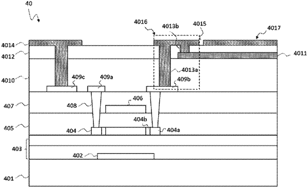
1. An array substrate, comprising:
a thin film transistor device, comprising a gate electrode, a source electrode, and a drain electrode;
an interface layer, covering the source electrode and the drain electrode, wherein the interface layer is composed of a nitride-oxide material and has a thickness less than a preset value;
a first transparent conductive layer, formed on the interface layer;
a passivation layer, formed on the interface layer and the first transparent conductive layer; and
a second transparent conductive layer, formed on the passivation layer, wherein the second transparent conductive layer comprises a drain electrode connection area and a conductive area, and the drain electrode connection area and the conductive area are electrically disconnected by a slit formed between the drain electrode connection area and the conductive area,
wherein the interface layer and the passivation layer are provided with a first via at a position corresponding to the drain electrode, the passivation layer is provided with a second via at a position corresponding to a portion of the first transparent conductive layer, and the second transparent conductive layer in the drain electrode connection area is electrically connected to the drain electrode through the first via and is electrically connected to the first transparent conductive layer through the second via.
|