| CPC H01L 27/088 (2013.01) [H01L 21/823456 (2013.01); H01L 21/823462 (2013.01); H01L 21/823468 (2013.01); H01L 29/40111 (2019.08); H01L 29/42376 (2013.01); H01L 29/4983 (2013.01); H01L 29/516 (2013.01); H01L 29/6656 (2013.01); H01L 29/6684 (2013.01); H01L 29/78391 (2014.09)] | 17 Claims |
|
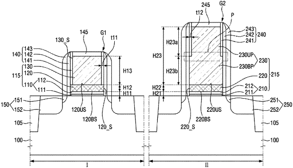
1. A semiconductor device, comprising:
a first gate electrode structure which includes a first gate insulating layer disposed on a substrate and a first gate electrode disposed on the first gate insulating layer;
a first spacer structure including a first spacer and a second spacer each disposed on side walls of the first gate electrode structure, the first spacer being disposed between the second spacer and the first gate electrode; and
a source/drain region disposed on opposite sides of the first gate electrode structure,
wherein the first gate electrode includes a lower part of the first gate electrode, an upper part of the first gate electrode disposed on the lower part of the first gate electrode,
wherein the first spacer is disposed on a side wall of the upper part of the first gate electrode and is omitted from a side wall of the lower part of the first gate electrode, and
wherein a width of the lower part of the first gate electrode is equal to a width of the upper part of the first gate electrode at a lowermost part of the first spacer.
|