| CPC H01L 27/088 (2013.01) [G01L 9/0042 (2013.01); G21C 17/00 (2013.01); H01L 23/49838 (2013.01); H01L 24/48 (2013.01); H01L 29/1608 (2013.01); H01L 2224/48227 (2013.01); H01L 2924/10272 (2013.01); H01L 2924/1424 (2013.01)] | 28 Claims |
|
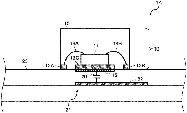
1. A radiation resistant circuit device, comprising:
a SiC semiconductor element equipped with a SiC integrated circuit;
a printed board on which the SiC semiconductor element is provided;
a conductive wiring and a covering material that are arranged inside the printed board, the conductive wiring having a predetermined surface facing a bottom surface of a substrate electrode of the SiC integrated circuit; and
an insulating material arranged between the bottom surface of the substrate electrode of the SiC integrated circuit and the predetermined surface of the conductive wiring;
wherein a parasitic capacitance is formed via the insulating material and the covering material between the bottom surface of the substrate electrode of the SiC integrated circuit and the conductive wiring.
|