| CPC H01L 27/0688 (2013.01) [G11C 5/06 (2013.01); H01L 21/8238 (2013.01); H01L 23/5384 (2013.01); H01L 23/5386 (2013.01); H01L 25/0657 (2013.01); H01L 27/092 (2013.01)] | 19 Claims |
|
1. A method, comprising:
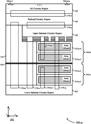
forming, based at least in part on doping portions of a first silicon substrate, a first plurality of transistors;
forming a first deck of memory cells above the first silicon substrate and coupled with the first plurality of transistors;
forming a second deck of memory cells above the first deck of memory cells;
bonding a second silicon substrate above the second deck of memory cells;
forming, based at least in part on doping portions of the second silicon substrate after bonding the second silicon substrate above the second deck of memory cells, a second plurality of transistors coupled with the second deck of memory cells; and
forming, after bonding the second silicon substrate above the second deck of memory cells, a first plurality of interconnects, wherein each interconnect couples one or more subsets of transistors of the first plurality of transistors with one or more subsets of transistors of the second plurality of transistors.
|