| CPC H01L 27/0292 (2013.01) [G06F 3/0412 (2013.01); G06F 3/04164 (2019.05); G09G 3/3266 (2013.01); G09G 3/3275 (2013.01); H10K 50/824 (2023.02); H10K 50/8426 (2023.02); H10K 59/122 (2023.02); H10K 59/126 (2023.02); H10K 59/131 (2023.02); H10K 59/40 (2023.02); G02F 1/13452 (2013.01); G02F 1/136204 (2013.01); G06F 3/044 (2013.01); G06F 3/0446 (2019.05); G06F 2203/04107 (2013.01); G09G 2310/0278 (2013.01); G09G 2310/0297 (2013.01); H10K 50/822 (2023.02); H10K 50/84 (2023.02); H10K 59/124 (2023.02); H10K 59/88 (2023.02)] | 20 Claims |
|
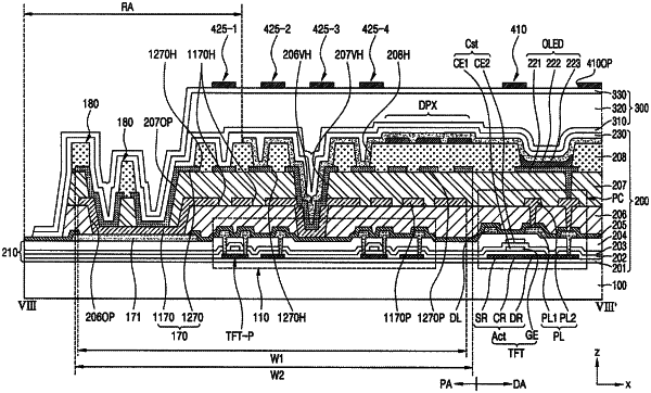
1. A display device, comprising:
a substrate including a display area and a peripheral area outside the display area;
a display element in the display area, the display element including a pixel electrode electrically connected to a thin film transistor, an opposite electrode of the pixel electrode, and an emission layer between the pixel electrode and the opposite electrode;
a peripheral circuit in the peripheral area;
a first shielding layer and a second shielding layer each located in the peripheral area;
an input sensor including sensing electrodes and signal lines, wherein
the sensing electrodes are located in the display area, and
the signal lines are connected to the sensing electrodes and located in the peripheral area; and
an encapsulation layer, wherein
in the peripheral area, the encapsulation layer is disposed between the first shielding layer and the signal lines, and the second shielding layer is disposed between the first shielding layer and the encapsulation layer, and
the first shielding layer has a plurality of first holes, the second shielding layer has a plurality of second holes, and the plurality of first holes and the plurality of second holes are arranged to be offset from each other in a plan view.
|