| CPC H01L 27/0255 (2013.01) [H01L 27/0266 (2013.01); H02H 9/046 (2013.01)] | 20 Claims |
|
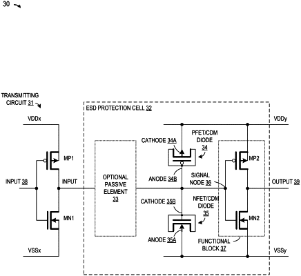
1. An integrated circuit, comprising:
a signal node coupled to receive an electrostatic discharge voltage from a transmitting circuit;
an electrostatic discharge protection circuit connected between a first voltage supply and a second voltage supply, comprising:
a first FinFET diode connected between the signal node and the first voltage supply, and
a second FinFET diode connected between the signal node and the second voltage supply; and
a protected circuit comprising a first FinFET operably coupled to the signal node that is protected against electrostatic discharge voltage damage by the electrostatic discharge protection circuit,
where the first and second FinFET diodes are each formed with a finFET device comprising (1) a body well region forming a first diode terminal connected to one of the first or second voltage supplies, and (2) shorted gate, source, and drain regions forming a second diode terminal connected to the signal node.
|