US 11,862,623 B2
Semiconductor device including source/drain contact having height below gate stack
Charles Chew-Yuen Young, Cupertino, CA (US); Chih-Liang Chen, Hsinchu (TW); Chih-Ming Lai, Hsinchu (TW); Jiann-Tyng Tzeng, Hsinchu (TW); Shun-Li Chen, Tainan (TW); Kam-Tou Sio, Hsinchu County (TW); Shih-Wei Peng, Hsinchu (TW); Chun-Kuang Chen, Hsinchu County (TW); and Ru-Gun Liu, Hsinchu County (TW)
Assigned to TAIWAN SEMICONDUCTOR MANUFACTURING CO., LTD., Hsinchu (TW)
Filed by TAIWAN SEMICONDUCTOR MANUFACTURING CO., LTD., Hsinchu (TW)
Filed on Feb. 10, 2023, as Appl. No. 18/167,651.
Application 18/167,651 is a division of application No. 17/092,100, filed on Nov. 6, 2020, granted, now 11,581,300.
Application 17/092,100 is a continuation of application No. 16/216,843, filed on Dec. 11, 2018, granted, now 10,833,061, issued on Nov. 10, 2020.
Application 16/216,843 is a continuation of application No. 15/159,692, filed on May 19, 2016, granted, now 10,177,133, issued on Jan. 8, 2019.
Application 15/159,692 is a continuation in part of application No. 14/280,196, filed on May 16, 2014, granted, now 9,478,636, issued on Oct. 25, 2016.
Prior Publication US 2023/0187434 A1, Jun. 15, 2023
Int. Cl. H01L 27/02 (2006.01); H01L 21/768 (2006.01); H01L 21/8234 (2006.01); H01L 23/485 (2006.01); G06F 30/394 (2020.01); H01L 23/528 (2006.01); H01L 29/66 (2006.01); H01L 21/84 (2006.01)
CPC H01L 27/0207 (2013.01) [G06F 30/394 (2020.01); H01L 21/76895 (2013.01); H01L 21/823418 (2013.01); H01L 21/823425 (2013.01); H01L 21/823431 (2013.01); H01L 21/823437 (2013.01); H01L 21/823475 (2013.01); H01L 23/485 (2013.01); H01L 21/76897 (2013.01); H01L 21/845 (2013.01); H01L 23/528 (2013.01); H01L 29/6656 (2013.01); H01L 29/6659 (2013.01); H01L 2924/0002 (2013.01)] 20 Claims
OG exemplary drawing
 
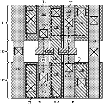
1. A method, comprising:
arranging a first gate structure extending continuously above a first active region and a second active region of a substrate;
arranging a first separation spacer disposed on the first gate structure to isolate an electronic signal transmitted through a first gate via and a second gate via that are disposed on the first gate structure, wherein the first gate via and the second gate via are arranged above the first active region and the second active region respectively; and
arranging a first local interconnect between the first active region and the second active region, wherein the first local interconnect is electrically coupled to a first contact disposed on the first active region and a second contact disposed on the second active region.