| CPC H01L 25/18 (2013.01) [H01L 23/481 (2013.01); H01L 23/5226 (2013.01); H01L 23/5286 (2013.01); H01L 24/08 (2013.01); H01L 24/16 (2013.01); H01L 27/016 (2013.01); H01L 28/90 (2013.01); H01L 2224/08147 (2013.01); H01L 2224/16147 (2013.01)] | 19 Claims |
|
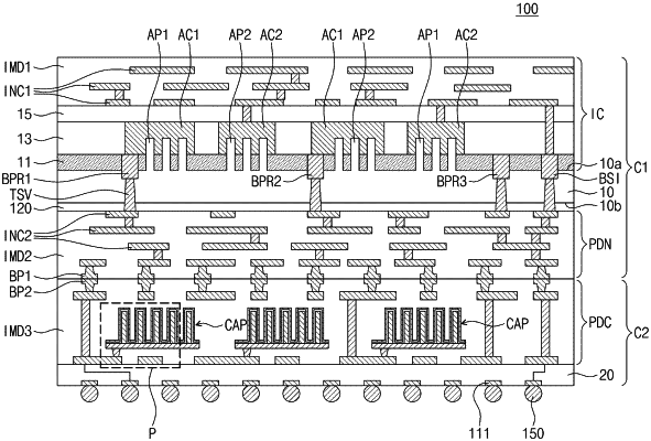
1. A semiconductor package, comprising:
a first semiconductor chip including a logic structure; and
a second semiconductor chip bonded to the first semiconductor chip,
wherein the first semiconductor chip comprises,
signal lines on a first surface of a first semiconductor substrate and connected to the logic structure,
a power delivery network on a second surface of the first semiconductor substrate, the second surface being opposite to the first surface, and
penetration vias penetrating the first semiconductor substrate and connecting the power delivery network to the logic structure,
wherein the second semiconductor chip comprises a capacitor layer that is on a second semiconductor substrate and is adjacent to the power delivery network,
wherein the logic structure comprises,
active patterns on the first surface of the first semiconductor substrate,
buried power rails in the first semiconductor substrate, and
active contacts connecting the buried power rails to the active patterns, and
wherein the penetration vias connects the buried power rails to the power delivery network.
|