| CPC H01L 25/0657 (2013.01) [H01L 23/481 (2013.01); H01L 24/05 (2013.01); H01L 24/06 (2013.01); H01L 24/08 (2013.01); H01L 24/16 (2013.01); H01L 24/32 (2013.01); H01L 24/73 (2013.01); H01L 25/0652 (2013.01); H01L 2224/05009 (2013.01); H01L 2224/06181 (2013.01); H01L 2224/08146 (2013.01); H01L 2224/16227 (2013.01); H01L 2224/32225 (2013.01); H01L 2224/73204 (2013.01); H01L 2225/06544 (2013.01)] | 20 Claims |
|
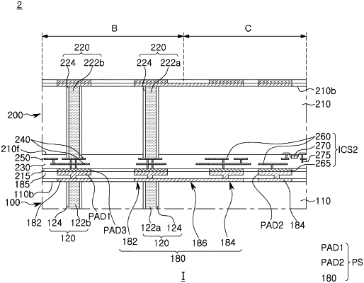
1. A semiconductor package comprising:
a first semiconductor chip; and
a second semiconductor chip disposed on the first semiconductor chip,
wherein the first semiconductor chip includes:
a first semiconductor body having a lower surface and an upper surface opposite each other;
an upper pad structure disposed on the upper surface of the first semiconductor body; and
a first through-electrode penetrating the first semiconductor body and electrically connected to the upper pad structure, and
the second semiconductor chip includes:
a second semiconductor body having a lower surface and an upper surface opposite each other;
lower bonding pads disposed on the lower surface of the second semiconductor body; and
an internal circuit structure including a connection pad pattern disposed at the same level as the lower bonding pads,
wherein:
the upper pad structure includes upper bonding pads and connection wirings,
the upper bonding pads are in contact with the lower bonding pads and the connection pad pattern,
the upper bonding pads include a first upper bonding pad overlapping the first through-electrode and a second upper bonding pad disposed in contact with the connection pad pattern, and
at least one of the connection wirings is electrically connected to the second upper bonding pad.
|