| CPC H01L 25/0657 (2013.01) [H01L 21/4803 (2013.01); H01L 21/4817 (2013.01); H01L 21/563 (2013.01); H01L 21/565 (2013.01); H01L 23/053 (2013.01); H01L 23/08 (2013.01); H01L 23/10 (2013.01); H01L 23/24 (2013.01); H01L 23/3142 (2013.01); H01L 23/367 (2013.01); H01L 23/3675 (2013.01); H01L 23/4334 (2013.01); H01L 23/3736 (2013.01); H01L 24/13 (2013.01); H01L 24/16 (2013.01); H01L 24/29 (2013.01); H01L 24/48 (2013.01); H01L 24/73 (2013.01); H01L 24/81 (2013.01); H01L 25/18 (2013.01); H01L 2224/1329 (2013.01); H01L 2224/13111 (2013.01); H01L 2224/13147 (2013.01); H01L 2224/13155 (2013.01); H01L 2224/16145 (2013.01); H01L 2224/16225 (2013.01); H01L 2224/16227 (2013.01); H01L 2224/2929 (2013.01); H01L 2224/29301 (2013.01); H01L 2224/29393 (2013.01); H01L 2224/48227 (2013.01); H01L 2224/73253 (2013.01); H01L 2224/81815 (2013.01); H01L 2225/06513 (2013.01); H01L 2225/06517 (2013.01); H01L 2225/06555 (2013.01); H01L 2225/06589 (2013.01); H01L 2924/1436 (2013.01); H01L 2924/1437 (2013.01); H01L 2924/1616 (2013.01); H01L 2924/16195 (2013.01); H01L 2924/16235 (2013.01); H01L 2924/16251 (2013.01); H01L 2924/173 (2013.01); H01L 2924/1715 (2013.01); H01L 2924/19041 (2013.01); H01L 2924/19105 (2013.01)] | 19 Claims |
|
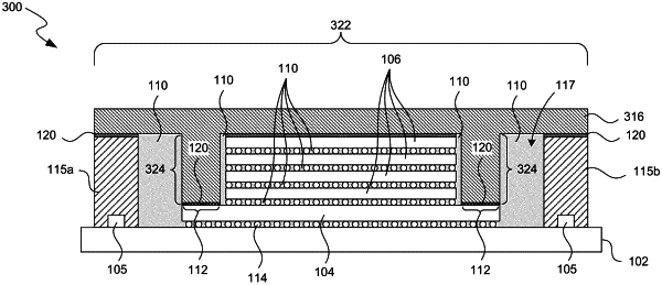
15. A semiconductor apparatus, comprising:
a base semiconductor die;
at least one semiconductor die stacked on top of the base semiconductor die;
a molded wall having parallel vertical surfaces on opposing sides of the at least one stacked semiconductor die and at least partially defining a cavity spaced apart from the at least one stacked semiconductor die, wherein the molded wall extends upward; and
a thermal lid and directly attached to a top portion of the molded wall, wherein
the thermal lid at least partially defines an upper boundary for the cavity and is configured to dissipate heat away from the first semiconductor die and the plurality of second semiconductor dies, and
the thermal lid includes at least two portions that protrude along different directions, wherein one of the two portions is directly attached to the base semiconductor die.
|