| CPC H01L 25/0652 (2013.01) [H01L 2225/0651 (2013.01); H01L 2225/06513 (2013.01); H01L 2225/06541 (2013.01); H01L 2225/06575 (2013.01); H01L 2225/06586 (2013.01); H01L 2225/06589 (2013.01)] | 18 Claims |
|
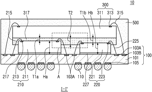
1. A semiconductor package comprising:
a package substrate;
a plurality of lower chip structures on the package substrate, the plurality of lower chip structures comprising a first chip structure having an upper surface at a first level and a second chip structure having an upper surface at a second level that is lower than that of the first level, wherein an upper surface of at least one of the plurality of lower chip structures is an active surface;
an upper chip structure on the plurality of lower chip structures and covering portions of upper surfaces of the plurality of lower chip structures;
a non-conductive adhesive layer on a lower surface of the upper chip structure and receiving upper portions of the plurality of lower chip structures, including the upper surface of the at least one of the plurality of lower chip structures that is the active surface, wherein the first chip structure extends into the non-conductive adhesive layer by a first depth that is greater than a second depth by which the second chip structure extends into the non-conductive adhesive layer; and
a molded member on the plurality of lower chip structures and the upper chip structure.
|