| CPC H01L 24/80 (2013.01) [H01L 21/565 (2013.01); H01L 23/4985 (2013.01); H01L 2224/80357 (2013.01); H01L 2224/83385 (2013.01); H01L 2924/1511 (2013.01); H01L 2924/15724 (2013.01); H01L 2924/15738 (2013.01)] | 22 Claims |
|
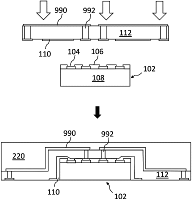
1. A method of forming a chip package, the method comprising:
providing a malleable carrier with a layer of an electrically conductive material formed thereon; and
positive fitting the malleable carrier to a chip to at least partially enclose the chip with the malleable carrier such that the malleable carrier conforms to outer edge sides of the chip,
wherein the layer at least partially physically contacts the chip, such that the layer electrically contacts a chip contact of the chip,
wherein the layer forms a redistribution layer.
|