| CPC H01L 24/20 (2013.01) [H01L 24/13 (2013.01); H01L 2224/2101 (2013.01); H01L 2224/214 (2013.01)] | 20 Claims |
|
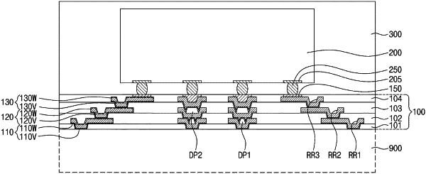
1. A semiconductor package, comprising:
a redistribution substrate;
a semiconductor chip on a first surface of the redistribution substrate, the semiconductor chip including a chip pad electrically connected to the redistribution substrate; and
a conductive terminal on a second surface, opposite the first surface, of the redistribution substrate,
wherein the redistribution substrate includes:
a first dielectric layer;
a second dielectric layer in contact with the first dielectric layer;
a first redistribution pattern in the first dielectric layer and the second dielectric layer;
a second redistribution pattern in the second dielectric layer; and
a insulative pattern formed in a first recess region of the first redistribution pattern,
wherein the first redistribution pattern is interposed between and electrically connects the chip pad and the second redistribution pattern,
wherein the first redistribution pattern, the second redistribution pattern and the insulative pattern are vertically overlapped.
|