| CPC H01L 24/19 (2013.01) [H01L 24/11 (2013.01); H01L 24/73 (2013.01); H01L 25/50 (2013.01); H01L 21/6836 (2013.01); H01L 25/0655 (2013.01); H01L 2224/73209 (2013.01); H01L 2924/014 (2013.01); H01L 2924/01028 (2013.01); H01L 2924/01029 (2013.01); H01L 2924/01079 (2013.01); H01L 2924/07025 (2013.01); H01L 2924/186 (2013.01); H01L 2924/3511 (2013.01); H01L 2924/37001 (2013.01)] | 10 Claims |
|
1. A packaging method for a fan-out wafer-level packaging structure, wherein the packaging method comprises:
providing two or more semiconductor chips, each of which has one or more pads, and bonding the semiconductor chips to a bonding layer to form a fan-out wafer array;
packaging the semiconductor chips by a plastic packaging layer;
removing the bonding layer, and forming a redistribution layer on the semiconductor chips to achieve interconnection between the semiconductor chips, wherein the redistribution layer comprises one or more redistribution sublayers stacked in sequence, wherein a first redistribution sublayer is in contact of the one or more pads;
wherein a method for forming each of the one or more redistribution sublayers comprises:
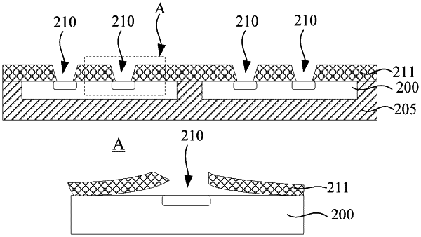
forming a dielectric layer on the semiconductor chips, wherein a warpage is generated in a forming process of the dielectric layer;
forming vias in the dielectric layer by photolithography;
baking the dielectric layer having the vias formed therein, wherein baking the dielectric layer eliminates the warpage on the dielectric layer around the vias;
curing the fan-out wafer array; and
forming a patterned metal distribution layer in the vias and on the dielectric layer, with the pattern of the patterned metal distribution layer corresponding to the layout of the vias;
and
forming metal bumps on the redistribution layer.
|