| CPC H01L 24/05 (2013.01) [H01L 24/03 (2013.01); H01L 24/11 (2013.01); H01L 24/13 (2013.01); H01L 24/16 (2013.01); H01L 2224/02379 (2013.01); H01L 2224/03462 (2013.01); H01L 2224/03464 (2013.01); H01L 2224/03828 (2013.01); H01L 2224/03829 (2013.01); H01L 2224/0401 (2013.01); H01L 2224/05541 (2013.01); H01L 2224/05547 (2013.01); H01L 2224/05559 (2013.01); H01L 2224/05573 (2013.01); H01L 2224/05582 (2013.01); H01L 2224/05611 (2013.01); H01L 2224/05639 (2013.01); H01L 2224/11334 (2013.01); H01L 2224/11849 (2013.01); H01L 2224/13006 (2013.01); H01L 2224/13111 (2013.01); H01L 2224/13139 (2013.01); H01L 2224/16225 (2013.01); H01L 2924/3512 (2013.01)] | 19 Claims |
|
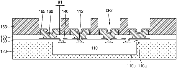
1. A method of manufacturing a wafer-level semiconductor package, the method comprising:
forming a redistribution layer and a passivation layer on a semiconductor chip;
etching a trench in an upper surface of the passivation layer;
forming a photoresist pattern having a first contact hole on the passivation layer such that the first contact hole is formed in a region corresponding to the trench in the upper surface of the passivation layer, and has a width wider than that of the trench in the upper surface of the passivation layer;
forming an under bump metal (UBM) in the first contact hole and the trench in the upper surface of the passivation layer such that the UBM is on the redistribution layer;
forming a preliminary solder layer covering the UBM surface; and
dropping a solder ball on the preliminary solder layer,
wherein at least one of the UBM and the preliminary solder layer is formed through an electroless plating method, and
wherein the thickness of the preliminary solder layer is approximately 1-50 μm.
|