| CPC H01L 23/562 (2013.01) [H01L 23/041 (2013.01); H01L 23/3128 (2013.01); H01L 23/49822 (2013.01); H01L 24/08 (2013.01); H01L 2224/08235 (2013.01)] | 20 Claims |
|
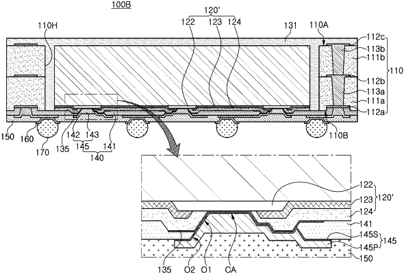
1. A method of manufacturing a semiconductor package, the method comprising:
preparing a semiconductor chip having an active surface on which contact pads are arranged, the semiconductor chip comprising a first insulating film disposed on the active surface and exposing the contact pads, and a second insulating film disposed on the first insulating film and comprising a first opening exposing connection regions of the contact pads,
forming a conductive crack preventing layer on the connection regions to extend onto a portion of the second insulating film around the first opening;
forming an insulating layer on the active surface of the semiconductor chip;
forming a second opening in the insulating layer, the second opening exposing a portion of the conductive crack preventing layer on the connection regions; and
forming a redistribution layer electrically connected to the connection regions through the second opening and extending onto the insulating layer.
|