| CPC H01L 23/562 (2013.01) [H01L 21/4825 (2013.01); H01L 21/565 (2013.01); H01L 23/3114 (2013.01); H01L 23/4952 (2013.01); H01L 23/49513 (2013.01); H01L 23/49548 (2013.01); H01L 23/49582 (2013.01)] | 20 Claims |
|
1. A method, comprising:
forming a semiconductor device by:
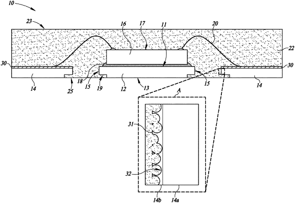
forming a conductive layer on a conductive substrate, the conductive layer including a plurality of microstructures at least partially embedded in the conductive layer;
forming a plurality of cavities in the conductive layer by removing the plurality of microstructures; and
at least partially filling the plurality of cavities with an encapsulation material.
|