| CPC H01L 23/562 (2013.01) [H01L 23/3114 (2013.01); H01L 23/3128 (2013.01); H01L 23/49816 (2013.01); H01L 24/09 (2013.01); H01L 24/17 (2013.01); H01L 24/19 (2013.01); H01L 24/20 (2013.01); H01L 21/568 (2013.01); H01L 24/13 (2013.01); H01L 2224/118 (2013.01); H01L 2224/13101 (2013.01); H01L 2224/18 (2013.01); H01L 2224/73204 (2013.01); H01L 2924/1431 (2013.01); H01L 2924/1433 (2013.01); H01L 2924/1436 (2013.01); H01L 2924/15174 (2013.01); H01L 2924/15311 (2013.01); H01L 2924/181 (2013.01); H01L 2924/18162 (2013.01); H01L 2924/3511 (2013.01)] | 20 Claims |
|
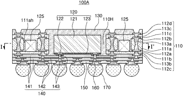
1. A semiconductor package comprising:
a connection member including a redistribution layer;
a semiconductor chip disposed on an upper surface of the connection member, and including an active surface on which a connection pad is disposed and an inactive surface opposing the active surface, the connection pad is electrically connected to the redistribution layer;
an encapsulant sealing at least a portion of the semiconductor chip;
a plurality of conductive structures disposed on a periphery of the semiconductor chip, extending in a direction perpendicular to the upper surface of the connection member within the encapsulant, and having one ends connected to the redistribution layer and other ends opposite to the one ends; and
at least one dummy structure disposed between first and second conductive structures adjacent to each other, among the plurality of conductive structures, and electrically insulated from the semiconductor chip and the plurality of conductive structures,
wherein the at least one dummy structure includes silicon,
wherein the at least one dummy structure is positioned on a lower level than the other ends of the plurality of conductive structures, and
wherein a maximum width of the at least one dummy structure is smaller than a separation distance between the first and second conductive structures.
|