US 11,862,572 B2
Laser-based redistribution and multi-stacked packages
ChangOh Kim, Incheon (KR); KyoungHee Park, Seoul (KR); SeongHwan Park, Incheon (KR); and JinHee Jung, Incheon (KR)
Assigned to STATS ChipPAC Pte. Ltd., Singapore (SG)
Filed by STATS ChipPAC Pte. Ltd., Singapore (SG)
Filed on Jan. 30, 2023, as Appl. No. 18/161,693.
Application 18/161,693 is a division of application No. 17/314,916, filed on May 7, 2021, granted, now 11,610,847.
Prior Publication US 2023/0170311 A1, Jun. 1, 2023
Int. Cl. H01L 23/552 (2006.01); H01L 23/66 (2006.01); H01L 21/56 (2006.01); H01L 23/31 (2006.01); H01L 21/48 (2006.01); H01Q 1/22 (2006.01)
CPC H01L 23/552 (2013.01) [H01L 21/486 (2013.01); H01L 21/56 (2013.01); H01L 23/31 (2013.01); H01L 23/66 (2013.01); H01Q 1/2283 (2013.01)] 25 Claims
OG exemplary drawing
 
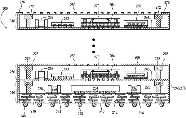
1. A semiconductor device, comprising:
a first package layer;
a first shielding layer formed over the first package layer, wherein the first shielding layer is patterned to form a redistribution layer;
an electrical component disposed over the redistribution layer;
an encapsulant deposited over the electrical component; and
a second shielding layer formed over the encapsulant, wherein the second shielding layer is patterned.