| CPC H01L 23/552 (2013.01) [H01L 23/498 (2013.01); H01L 25/00 (2013.01)] | 20 Claims |
|
1. A semiconductor package, comprising:
a package substrate including a first surface and a second surface facing each other;
a semiconductor chip on the first surface of the package substrate;
a capping insulation layer covering an upper surface and a side surface of the semiconductor chip;
a shielding layer covering an upper surface and a side surface of the capping insulation layer;
a mold layer covering an upper surface and a side surface of the shielding layer; and
a plurality of external connection terminals provided on the second surface of the package substrate,
wherein:
the package substrate includes a first region that vertically overlaps with the semiconductor chip and a second region that surrounds the first region,
at least some of the external connection terminals are provided on the second region of the package substrate,
the capping insulation layer is in contact with the upper surface and the side surface of the semiconductor chip,
the shielding layer is in contact with the upper surface and the side surface of the capping insulation layer,
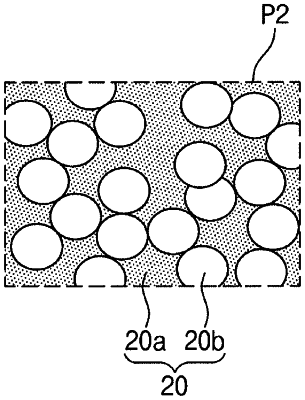
the capping insulation layer includes a polymer-containing layer and insulating particles dispersed therein,
the shielding layer includes at least one metal layer, and
a thickness of the mold layer is greater than a thickness of the capping insulation layer.
|