| CPC H01L 23/5385 (2013.01) [H01L 21/4846 (2013.01); H01L 23/49833 (2013.01); H01L 23/5389 (2013.01); H01L 25/105 (2013.01); H01L 25/18 (2013.01); H01L 23/49827 (2013.01); H01L 2225/107 (2013.01); H01L 2225/1023 (2013.01); H01L 2225/1035 (2013.01); H01L 2225/1041 (2013.01); H01L 2225/1058 (2013.01)] | 20 Claims |
|
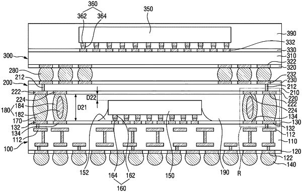
1. A semiconductor package comprising:
a substrate including a first insulating layer, first conductive patterns in the first insulating layer, an upper passivation film, first upper pads, and second upper pads;
an interposer disposed on a top surface of the substrate and including a second insulating layer and second conductive patterns in the second insulating layer;
connecting members in contact with the top surface of the substrate and a bottom surface of the interposer; and
supporting members including solder parts which are in contact with the top surface of the substrate and the bottom surface of the interposer, and core parts which are disposed in the solder parts and include a different material from the solder parts,
wherein the upper passivation film, the first upper pads, and the second upper pads are formed on a top surface of the first insulating layer, the first upper pads in contact with the connecting members, and the second upper pads in contact with the supporting members,
wherein the upper passivation film covers at least parts of the first upper pads and the second upper pads so as to include a top surface that is at a higher vertical level in a direction perpendicular to the top surface of the substrate than top surfaces of the first upper pads and the second upper pads,
wherein the connecting members electrically connect the first conductive patterns and the second conductive patterns, and
wherein the supporting members do not electrically connect the first conductive patterns and the second conductive patterns.
|