| CPC H01L 23/535 (2013.01) [G06F 30/394 (2020.01); H01L 21/486 (2013.01); H01L 21/4846 (2013.01); H01L 21/76895 (2013.01); H01L 23/498 (2013.01); H01L 23/49827 (2013.01); H01L 27/0207 (2013.01); H01L 27/11807 (2013.01); H01L 2027/11875 (2013.01)] | 20 Claims |
|
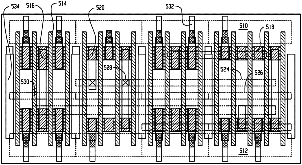
1. A multi-layer semiconductor device structure in an integrated circuit (IC) comprising:
a plurality of cells arranged on a substrate and fabricated using a fabrication technology having a metal-0 oxide diffusion (M0OD) layer and a polysilicon (PO) layer;
an input port fabricated on the M0OD or PO layer of a first cell of the plurality of cells;
an output port fabricated on the M0OD layer of a second cell of the plurality of cells;
a metal-1 layer over the input and output ports, the metal-1 layer having a first set of metal-1 conduction paths and a second set of metal-1 conduction paths, wherein at least one metal-1 conduction path in the first set of metal-1 conduction paths extends across multiple cells; and
a metal-2 layer having horizontal direction metal-2 conduction paths over the metal-1 layer, wherein the metal-2 conduction paths are in a direction perpendicular to the direction of the metal-1 conduction paths, the metal-2 layer having a first set of metal-2 conduction paths and a second set of metal-2 conduction paths;
wherein the first set of metal-1 conduction paths and the first set of metal-2 conduction paths are configured to interconnect circuit components in different cells, wherein inter cell connections in the semiconductor device structure are made using the first set of metal-1 conduction paths or a combination of the first set of metal-1 and the metal-2 conduction paths.
|