| CPC H01L 23/535 (2013.01) [C22C 30/00 (2013.01); H01L 21/2855 (2013.01); H01L 21/28518 (2013.01); H01L 21/76805 (2013.01); H01L 21/76843 (2013.01); H01L 21/76846 (2013.01); H01L 21/76858 (2013.01); H01L 21/76864 (2013.01); H01L 21/76895 (2013.01); H01L 23/485 (2013.01); H01L 23/53223 (2013.01); H01L 23/53266 (2013.01); H01L 29/7851 (2013.01); H01L 23/53209 (2013.01); H01L 23/53238 (2013.01); H01L 23/53252 (2013.01)] | 20 Claims |
|
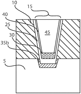
1. A method of forming a contact to a semiconductor device comprising:
forming a nickel platinum semiconductor alloy on a silicon contact;
depositing a titanium layer having an angstrom scale thickness in contact with the nickel platinum semiconductor alloy;
forming an aluminum containing fill on the titanium layer;
forming a metal nitride layer and metal containing contact to complete a material stack beginning with the nickel platinum semiconductor alloy; and
applying anneal after at least said depositing the titanium layer to the material stack to provide a contact alloy comprising nickel, platinum, aluminum, titanium and a semiconductor element from the contact surface of the semiconductor device, the contact alloy comprising nickel (Ni) ranging from 20 at. % to 30 at. %, platinum (Pt) ranging from 0 at. % to 10 at. %, aluminum (Al) ranging from 40 at. % to 60 at. %, and silicon (Si) ranging from 5 at. % to 20 at. %.
|