| CPC H01L 23/535 (2013.01) [H01L 21/76805 (2013.01); H01L 21/76895 (2013.01); H10B 43/27 (2023.02); H10B 43/40 (2023.02)] | 20 Claims |
|
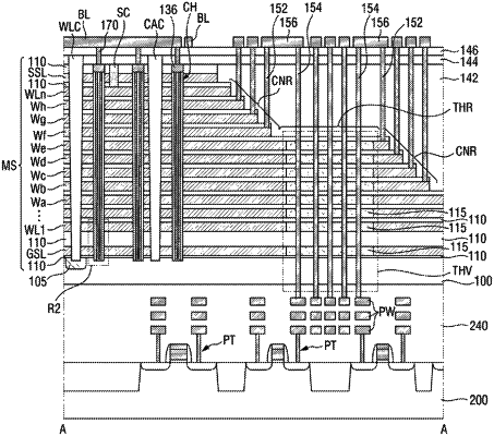
1. A semiconductor device, comprising:
a cell array region and an extension region arranged along a first direction, wherein contact regions and through regions are alternately arranged along the first direction in the extension region;
a mold structure including a plurality of first insulating patterns and a plurality of gate electrodes, which are alternately stacked on a first substrate;
a channel structure penetrating the mold structure in the cell array region to intersect the plurality of gate electrodes;
respective gate contacts in the contact regions, wherein the respective gate contacts are on the mold structure and are connected to each of the gate electrodes; and
a plurality of second insulating patterns that are stacked alternately with the plurality of first insulating patterns in the mold structure in the through regions, the plurality of second insulating patterns including a different material from the plurality of first insulating patterns.
|