| CPC H01L 23/535 (2013.01) [H01L 21/3212 (2013.01); H01L 21/7684 (2013.01); H01L 21/76805 (2013.01); H01L 21/76843 (2013.01); H01L 21/76895 (2013.01); H10B 41/27 (2023.02); H10B 41/35 (2023.02); H10B 43/27 (2023.02); H10B 43/35 (2023.02)] | 5 Claims |
|
1. A three-dimensional (3D) memory structure, comprising:
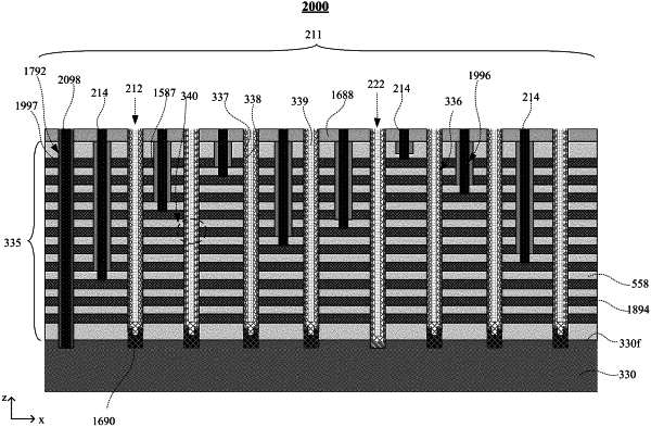
a film stack comprising conductive and dielectric layers alternatingly stacked on top of each other in a first direction;
a common source contact penetrating the film stack in the first direction;
memory strings in a channel structure region penetrating through the film stack in the first direction, wherein each of the memory strings comprises a memory film and a channel layer;
contact structures in the channel structure region penetrating through one or more of the conductive and dielectric layers in the first direction such that a respective conductive layer of the film stack is electrically connected to at least one of the contact structures; and
dummy memory strings adjacent to the contact structures and penetrating through the film stack in the first direction, each of the dummy memory strings comprising a core filling film, wherein:
each of the contact structures comprises a liner surrounding a conductive material;
the conductive material contacts the respective conductive layer of the film stack;
the liner comprises an insulator configured to electrically isolate the contact structures from one or more conductive layers of the film stack in a second direction perpendicular to the first direction and is distant from the respective conductive layer of the film stack in the first direction;
at least one memory string is directly adjacent to two contact structures that are on opposite sides of the at least one memory string in the second direction; and
the common source contact comprises an isolation liner configured to electrically isolate the common source contact from the conductive layers of the film stack.
|