| CPC H01L 23/5283 (2013.01) [H01L 21/76816 (2013.01); H01L 21/76877 (2013.01); H01L 23/5226 (2013.01); H10B 41/10 (2023.02); H10B 41/27 (2023.02); H10B 43/10 (2023.02); H10B 43/27 (2023.02)] | 20 Claims |

|
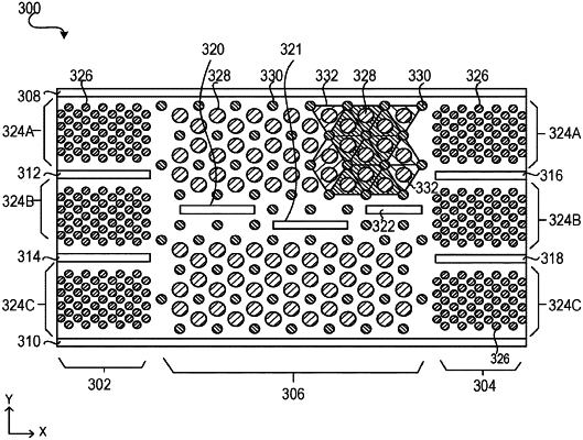
1. A semiconductor device, comprising:
a substrate;
a stack of word line layers and insulating layers that are stacked alternatingly over the substrate; and
channel structures formed in a first array region and a second array region of the stack, the first and second array regions being positioned at two opposing sides of the stack, wherein
a first staircase is formed in a connection region of the stack that is arranged between the first array region and the second array region, the first staircase having non-quadrilateral treads,
a second staircase is formed in the connection region of the stack, the second staircase having non-quadrilateral treads, and
the connection region in the stack includes a separation region positioned between the first and second staircases.
|