| CPC H01L 23/5226 (2013.01) [H01L 23/53209 (2013.01); H01L 23/53295 (2013.01); H01L 29/1033 (2013.01)] | 20 Claims |
|
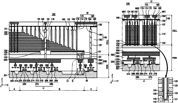
1. A semiconductor device, comprising:
a peripheral circuit region including
a first substrate,
circuit devices provided on the first substrate, and
a first interconnection structure electrically connected to the circuit devices;
a memory cell region including
a second substrate disposed on an upper portion of the first substrate and having a first region and a second region,
gate electrodes spaced apart from each other and stacked in a first direction perpendicular to an upper surface of the second substrate in the first region and extending while having a staircase form in a second direction perpendicular to the first direction in the second region,
interlayer insulating layers alternately stacked with the gate electrodes,
channel structures penetrating the gate electrodes, extending in the first direction, and including a channel layer, and
a second interconnection structure electrically connected to the gate electrodes and the channel structures; and
a third interconnection structure including
an upper via filling a via hole with the same material as the second substrate and including a barrier layer covering an internal side wall and a bottom surface of the via hole and a semiconductor layer disposed on the barrier layer, and
a lower interconnection structure connected to a lower portion of the upper via and having a structure corresponding to the first interconnection structure.
|