| CPC H01L 23/5226 (2013.01) [H01L 23/5283 (2013.01); H10B 41/27 (2023.02); H10B 41/35 (2023.02); H10B 41/41 (2023.02); H10B 43/27 (2023.02); H10B 43/35 (2023.02); H10B 43/40 (2023.02); H10B 63/84 (2023.02)] | 10 Claims |
|
1. A semiconductor device comprising:
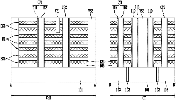
a stack structure including a plurality of interlayer insulating layers and a plurality of gate conductive layers, which are stacked in an alternating manner;
a first vertical structure penetrating a portion of the gate conductive layers and a portion of the interlayer insulating layers in a substantially vertical manner, the portion of the gate conductive layers and the portion of the interlayer insulating layers being disposed at an upper end portion of the stack structure, wherein the first vertical structure is formed in a cell region, and wherein the first vertical structure is formed of an oxide layer;
at least one support structure being formed of the same material as the first vertical structure, wherein the at least one support structure is formed of the oxide laver, and wherein the at least one support structure is formed in a contact region and penetrates the stack structure in a substantially vertical manner;
a first barrier layer over a sidewall of each of the at least one support structure;
a contact plug penetrating the stack structure in a substantially vertical manner, the contact plug being formed in the contact region;
a source line layer and a contact pad that are disposed on a bottom of the stack structure, the contact plug being connected to the contact pad, the at least one support structure being in contact with the source line layer; and
an isolation layer placed between the source line layer and the contact pad,
the isolation layer separating the source line layer and the contact pad.
|